HomeResearchResearch Lines
Materials and Processes for Electronics

						Research objectives and activities

O4.1) Development of scalable techniques for the integration of graphene and other 2D materials in microelectronic devices.

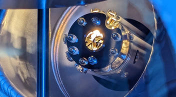
One of our objectives is to scale up 2D materials production to meet the large area demands of the microelectronic industry. A newly acquired MBE system (financed by the PERTE-Chip) will facilitate the development of epitaxial graphene and other 2D semiconductors on large-area substrates.

O4.2) Semiconducting memristive materials based on ionic transport for neuromorphic technologies. Memory resistors (memristors) are fundamental components in resistive switching devices with memory capabilities. They require much less energy to operate and are faster than current solid-state storage technologies. The current state of the art relies on metal oxides or phase transition materials, but they exhibit limited flexibility and are prone to structural rigidity. At ICMol we have developed a hybrid molecular-based memristive nanocomposite (Adv.Elect.Mat. 2022, 8, 2101192). These hybrid memristors will be electrically characterized and memristive devices will be fabricated. This involves from the memristive circuits preparation to the fabrication of modules based on this circuit.

O4.3) Thin film semiconductor deposition process by vapor transport and integration into transistors.

Perovskite offer potential advantages over current thin-film transistor (TFT) materials (metal oxides) due to their high charge mobility exceeding 100 cm2/(Vs). However, progress in utilizing perovskite channels for high-performance transistors has been hindered by ion migration (hysteresis), resulting in reduced effective mobility. Vapor-deposited perovskite films present reduced ionic charge density, leading to nearly hysteresis-free optoelectronic devices (ACS Energy Lett. 2017, 2, 1214), while enabling precise thickness control of perovskite films and compatibility with various substrates. We are engaged in developing perovskite thin films for TFT channels, employing highly crystalline hybrid or fully inorganic perovskites.

O4.4) LED devices. The group of Bolink has been on the forefront of perovskite-based LEDs, demonstrating room temperature electroluminescence in 2014. In the past the activities were focused on solution processed perovskites and their integration into LEDs (record efficiency 22 %). We will now focus on the development of highly efficient luminescent perovskite prepared by vacuum sublimation.

O4.5) Photodetectors.

In the last 3 years we have fabricated perovskite photodetectors using dry processing methods (Adv.Opt.Mater. 2022, 18, 2201047; J.Mater.Chem. C 2023, 11, 1258).

We now plan to extend the detection capabilities to two regions of extreme interest for ICT industry and the biomedical sector.


